Creating a PCB: The Toru Bhai Style
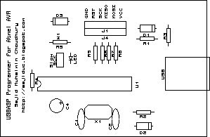
Today, I went to make the PCB of my AVR USB Programmer (USBASP). BUET Students usually go to 'Toru Bhai' for making PCBs. I did my design in Proteus Isis and Ares. I talked to Toru Bhai, and he asked me to bring print out of the masks I designed. Basically 3 masks are required for single layer PCB:
Bottom Copper


Although, Toru Bhai is reluctant to do the Solder Resist, as he claims it is too expensive. As I went today in his 'factory', in 6/1/F, Ram Krishna Mission Road, he didn't have much work load and insisted me to wait and take my PCB with me. So I watched the fabrication process. Surprisingly, the screen printing is very much similar to VLSI fabrication.

Fitting the screen


Grinder used to smoothen the sides


Top Components (Silk Screen)

Solder Resist

Although, Toru Bhai is reluctant to do the Solder Resist, as he claims it is too expensive. As I went today in his 'factory', in 6/1/F, Ram Krishna Mission Road, he didn't have much work load and insisted me to wait and take my PCB with me. So I watched the fabrication process. Surprisingly, the screen printing is very much similar to VLSI fabrication.
Basically, a thin fabric with tiny holes in it is first covered in paint, and the tracing paper with the print out of the pattern is held in front of it. The screen is enclosed in glass, and exposed to solar light. The region covered by ink in the tracing paper remain unchanged, but the region exposed to light hardened. The screen is then washed, and the region covered by ink on tracing paper during solar exposure has its paint removed.
Then the screen is used to imprint the pattern of the tracing paper on copper board. The paint has to be insoluble to water. After the print, the board is submerged to FeCl3 (Ferric Chloride). Regions not covered by paint has its copper removed, as Copper reacts with FeCl3 to produce Cu-Chloride.
Afterwards, the paint is removed. Then holes are drilled to it, and the top layer patterns are drawn accordingly.
I got some pictures of the process:
The lab:

A screen looks like this:


Fitting the screen

Screen ready for action

Patternizing

FeCl3 Etching

Drilling Holes

Grinder used to smoothen the sides


. BUET Students usually go to 'Toru Bhai' for making PCBs. I did my...)
n1 gud....
ReplyDeleteDude as u used Proteus ares i am facing problem in that as when i place ground plane in the ckt there is certain area which lefts out everytime.....
trying from last 3 days...still i cant get rid off.
so please help me
thnx in advance
Dude, Actually I'm an armature PCB designer. I haven't used ground plane.
ReplyDeleteHow did you create the solder resist, i cant quite work out how to do it.
ReplyDeleteHi. Sajid
ReplyDeleteIm from Tunisia and im interresting by your pcb making process...
-is this method is economic in comparaison of the other?
-its applicable on Double side pcb?
-how cost ferric chloride and copper laminate PCB on Bengladesh (in $)?
THANKS.
Hi Dali,
ReplyDeleteTechnically the process is not mine. It is widely used in Bangladesh and arguably, in the rest of the world. I think Ferric Chloride cost about 150 Taka/KG (70Taka=1USD) 2-3 years ago. I am not sure about the current price.
Help, we don't have his number. What is Toru bhai's mobile number?
ReplyDelete