ADC Interfacing of AVR (ATmega32)
The Analogue to Digital Converter of the Atmel AVR Microcontroller was one of the main reasons of me choosing it over the cheap AT89S52 microcontroller.
As mentioned in my previous blog post, I had recently given a workshop at the AIUB along with my friend Omee. Due to time shortage, I could not finish my presentation on ADCs. I wanted to share some of the materials that I studied here in my blog post.
In short the ADC converts the voltage level measured at a ADC channel pin to a corresponding binary value. The converted value is stored in a 16 bit register ADC which is divided into two segments: ADCH and ADCL.
Firstly, the ADC of the ATmega32, or most AVR microcontrollers is 10 bit. That means there are 2^10 or 1024 levels detectable by this ADC which are uniformly spaced over the region of the maximum and minimum voltage level. The minimum voltage is 0V, and maximum is either Vcc or internally generated 2.56V.

Before using the ADC it must be preconfigured. The ADC has 8 channels, that can be selected from the ADMUX register. This is the structure of the ADMUX register:


The ADMUX register also has a ADLAR bit, which can Left Adjust or right adjust the output of the ADC. This shows the effect of changing ADLAR bit value in ADC:

So depending on operation, if the least significant bits can be discarded, and not much accuracy is needed, ADLAR=1 can be used and ADCH value can just be taken readily.
Also the reference voltage of ADC is selected by the REFS1 and REFS0 bits. It can be used to select an externally generated Vref, as well as the 2.56V internally generated voltage.

For some other control of the ADCs, there are some extra registers: ADC Control and Status Register. Funny thing is, the register structure is different in ATmega8 and ATmega32, so while this post highlights only ATmega32 microcontroller, it is suggested that you should always consult datasheet before writing your code for a specific microcontroller.
The ADC can be configured to fire up automatically, so that it converts the value and at the end of conversion, generates an interrupt. These settings are also in the control and status register

ADEN bit sets the ADC enabled.
ADATE - ADC Auto Trigger Enable, if set it will automatically do the conversion based on the triggering condition (discussed later)
ADIF - ADC Interrupt Flag
ADIE - ADC Interrupt Enable - Triggers Interrupt on completed conversion, works when global interrupt is enabled.
ADPS2-0 - these select the clock frequency of the trigger after which the ADC is triggered. F_CPU is divided by the division factor based on these:
 SFIOR Register (Also termed as ADCSRB in some microcontrollers) has the function of setting the condition on which the ADC is triggered. For free running mode, it always trigger at the specified clock cycle. For other modes, it can be configured to be triggered at a particular hardware condition or timer or counter condition.


For the ADC to work properly, it requires some time duration. That is shown in the table:

 It is easy to avoid the division in ADC by using the internal 2.56 V. By using this value we can calculate that
ADC = Vin * 400. So Vin = ADC / 400.
To further illustrate the example, the voltage from a temperature sensor LM35 is sensed with the ADC. The LM35 gives a voltage of 10mV per degree celsius. So the voltage output = 0.01 V * temperature.
So if we measure the value of the ADC, we know that Vin = ADC/400, and again Vin = 0.01 * Temp
So 0.01 * Temp = ADC/400, or Temp = ADC / 400 / 0.01 = ADC / 4
So the temperature is just the measured value of the ADC divided by 4. Since division by 4 can be accomplished by a right shift of 2 binary digits, it can be done quite computationally efficiently.
This is the model of LM35 IC in proteus. The Temperature is set in the model with the up and down arrows.

As mentioned in my previous blog post, I had recently given a workshop at the AIUB along with my friend Omee. Due to time shortage, I could not finish my presentation on ADCs. I wanted to share some of the materials that I studied here in my blog post.
In short the ADC converts the voltage level measured at a ADC channel pin to a corresponding binary value. The converted value is stored in a 16 bit register ADC which is divided into two segments: ADCH and ADCL.
Firstly, the ADC of the ATmega32, or most AVR microcontrollers is 10 bit. That means there are 2^10 or 1024 levels detectable by this ADC which are uniformly spaced over the region of the maximum and minimum voltage level. The minimum voltage is 0V, and maximum is either Vcc or internally generated 2.56V.

Before using the ADC it must be preconfigured. The ADC has 8 channels, that can be selected from the ADMUX register. This is the structure of the ADMUX register:
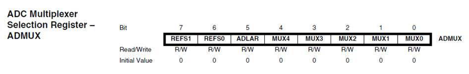


So depending on operation, if the least significant bits can be discarded, and not much accuracy is needed, ADLAR=1 can be used and ADCH value can just be taken readily.
Also the reference voltage of ADC is selected by the REFS1 and REFS0 bits. It can be used to select an externally generated Vref, as well as the 2.56V internally generated voltage.

For some other control of the ADCs, there are some extra registers: ADC Control and Status Register. Funny thing is, the register structure is different in ATmega8 and ATmega32, so while this post highlights only ATmega32 microcontroller, it is suggested that you should always consult datasheet before writing your code for a specific microcontroller.
The ADC can be configured to fire up automatically, so that it converts the value and at the end of conversion, generates an interrupt. These settings are also in the control and status register

ADEN bit sets the ADC enabled.
ADATE - ADC Auto Trigger Enable, if set it will automatically do the conversion based on the triggering condition (discussed later)
ADIF - ADC Interrupt Flag
ADIE - ADC Interrupt Enable - Triggers Interrupt on completed conversion, works when global interrupt is enabled.
ADPS2-0 - these select the clock frequency of the trigger after which the ADC is triggered. F_CPU is divided by the division factor based on these:


For the 10 bit ADC, the value stored in register is given by:

ADC = Vin * 400. So Vin = ADC / 400.
To further illustrate the example, the voltage from a temperature sensor LM35 is sensed with the ADC. The LM35 gives a voltage of 10mV per degree celsius. So the voltage output = 0.01 V * temperature.
So if we measure the value of the ADC, we know that Vin = ADC/400, and again Vin = 0.01 * Temp
So 0.01 * Temp = ADC/400, or Temp = ADC / 400 / 0.01 = ADC / 4
So the temperature is just the measured value of the ADC divided by 4. Since division by 4 can be accomplished by a right shift of 2 binary digits, it can be done quite computationally efficiently.
This is the model of LM35 IC in proteus. The Temperature is set in the model with the up and down arrows.

I have used the circuit of the previous blog post identically, just adding temp to the PA0 pin.
    #include <avr/io.h>
#include <util/delay.h>
#include <avr/interrupt.h>

/* Code for single pin addressing */
typedef struct
{
  unsigned char bit0:1;
  unsigned char bit1:1;
  unsigned char bit2:1;
  unsigned char bit3:1;
  unsigned char bit4:1;
  unsigned char bit5:1;
  unsigned char bit6:1;
  unsigned char bit7:1;
}io_reg;

#define D0      ((volatile io_reg*)_SFR_MEM_ADDR(PORTA))->bit4
#define D1      ((volatile io_reg*)_SFR_MEM_ADDR(PORTA))->bit5

/* Code for 7 seg display */
static unsigned  char SEVEN_SEG[] = {
0x3F,
0x06,
0x5B,
0x4F,
0x66,
0x6D,
0x7D,
0x07,
0x7F,
0x6F,
0x77,
0x7C,
0x39,
0x5E,
0x79,
0x71};

volatile int temperature;
volatile char garbage;

ISR(ADC_vect) {
temperature = ADCL>>2; /*collect sample from ADC */
garbage = ADCL;
garbage= ADCH;

}


int main (void) {

int delay = 1000;
int i=0;
DDRB = 0xFF;
DDRA |= 0b11110000;

DDRD &= 0x00;
DDRC = 0xFF;
PORTC = 0x00;
//DDRD = 0x00;


/* adc initialization */
ADCSRA |= (1 << ADPS1) | (1 << ADPS0);
ADMUX |= (1 << REFS1) | (1 << REFS0);


//Set ADC to free run mode
   SFIOR &= ~((1 << ADTS2) | (1 << ADTS1) | (1 << ADTS0));

   // Enables ADC for use
   ADCSRA |= (1 << ADEN);

   // Enable ADC Interrupt
   ADCSRA |= (1 << ADIE);

   // ADC Auto Trigger Enable
   ADCSRA |= (1 << ADATE);

   // Enable Global Interrupts
   sei();

   // Starts ADC conversion
   ADCSRA |= (1 << ADSC);


while (1) {


//show number in decimal

D0 = 0;
D1 = 0;
PORTB = SEVEN_SEG[temperature/10];
D0 = 0;
D1 = 1;
while (++i < delay);

D0 = 0;
D1 = 0;
PORTB = SEVEN_SEG[temperature%10];
D0 = 1;
D1 = 0;
while (--i > 0);


}
}
The final output is shown here.


There is a mistake in one of the formulae presented.
ReplyDeleteThe correct formula should be:
ADC = (Vin * 1023)/Vref
Not 1024, since there are 1024 levels and 0 is also a level and thus maximum level/value is 1023.
Tahmid.
Actually the formula was taken from the data sheet of ATmega32 (page 213). I think the ADC is designed to take that formula in particular, as multiplications for post processing becomes easier if one of the number is a power of 2.
DeleteDear Sajid, I'm glad to see your profile and impressed, I need your help can you send me make a PCB board and also tell me where put charging and battery full indication LED. part as per blow:
ReplyDeleteThis is auto 6V battery charger parts Items:
1. IC : LM317T IC Qty. 1
2. Diode : 1N4007 Qty. 5
3. Zener Diode : 6.8/0.5W Qty.1
4. Capacitor : 25V 1000uF Qty. 1
5. Variable Resistor : 2.2K Qty. 1
6. Resistance : 16 Ohm/5W Qty.1
7. Resistance : 1.2 Ohm Qty.1
8. Resistance : 180 Ohm Qty.1
9. Transistor : BC548 Qty.1
10. Transformer 230VAC : 0-9V / 500mA Qty.1
Hello Mr.S.M.Caoudhury have any email id where i can send u any query if is possible pls send me on my id roseofcanada401@gmail.com
ReplyDeleteThanks
from Toor B.
Nice description. Thanks.
ReplyDeleteYou have put together the most important parts of the AD-Setup Options. You could also write something about Clocksetup of the AD
Hello Sajid Muhaimin Choudhury. Indeed great project. :-) :-) But temperature is showing 0 for negative values in LM35 and after 64 degree in LM35 temp. is also showing 0. Please check and inform if you can edit the code to overcome these limitations. Hoping your reply. Please mail me at sanjeeb2008mohanty@gmail.com
ReplyDeleteI teach two courses at Cornell University in Electrical and computer engineering. Recently I have uploaded a full set of lectures for each course to YouTubeEDU. The lectures have comments which link to lab exercises and other supportingMaterial.
ReplyDeleteThe general YouTube channel is
https://www.youtube.com/user/ece4760
Microcontroller lectures from Cornell university are at
https://www.youtube.com/course?list=ECD7F7ED1F3505D8D5
and student projects at
https://www.youtube.com/playlist?list=PLEB09A7C8641987A8&feature=plcp
Full documentation at
http://people.ece.cornell.edu/land/courses/ece4760/
and
http://people.ece.cornell.edu/land/courses/ece4760/FinalProjects/
Field Programmable Gate Array lectures from Cornell university are at
https://www.youtube.com/course?list=EC2BA78454E71FF0E5
and projects at
https://www.youtube.com/playlist?list=PL2E0D05BEC0140F13&feature=plcp
full docs at
http://people.ece.cornell.edu/land/courses/ece5760/
and
http://people.ece.cornell.edu/land/courses/ece5760/FinalProjects/
Perhaps they would be useful on your site.
Thanks.
Outstanding, thanks. I'm glad I stumbled across this.
DeleteThank for the code! its really helpful. very clean and neat explanation
ReplyDeletehttp://www.npeducations.com
Thank for the code! its really helpful. very clean and neat explanation
ReplyDeletecan i use 230 v ac in adc channel at atmega16
ReplyDeletehi
ReplyDeletecan i copy this code
please help me..
কানও রেফারেন্স ভল্ট সিলেক্ট করতে হয় ?
ReplyDelete